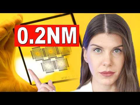
The development of computer chips is on the verge of a significant breakthrough, with the potential to produce 0.2nm chips by 2037, which will revolutionize technology and enable more powerful and compact chips for applications such as AI
Questions to inspire discussion
Future Chip Architecture
🔄 Q: What is the next big shift in computer chip technology?
A: The transition from gate-all-around to CFET architecture, enabling single Ångström dimension scaling and unlocking the next level of performance.
⚡ Q: How will backside power delivery in CFET architecture improve chip performance?
A: It will free up space on top for signaling and interconnecting logic gates, leading to faster computing and more efficient power consumption.
Advanced Materials and Design
🧪 Q: Why are carbon nanotubes (CNTs) being explored for future chip technology?
A: CNTs offer high speed and current at low voltages, but researchers must overcome the big problem of leakage power when idle.
🧩 0 concept in chip design? A: It involves building chips in different layers with specific jobs, using the best material and technology for each layer (e.g., AI, graphics) to improve scaling and reduce complexity.
Memory Solutions
💾 Q: How can CFET architecture address SRAM memory bottlenecks?
A: CFET can fit SRAM layout well and provide a decent jump in density, while 3D stacking becomes necessary to address the memory wall in DRAM.
Industry Dynamics
💼 Q: How is competition driving progress in chip manufacturing?
A: Healthy competition between companies like TSMC, Samsung, and Intel is driving progress and helping keep prices affordable for devices and AI services, despite increasing manufacturing complexity and costs.
Key Insights
Transistor Technology Advancements
🔬 Transistors, the nanoscopic switches that form the building blocks of computer chips, are driving the entire digital world by turning on and off billions of times per second.
💡 The CFET architecture, involving stacked gate-all-around devices in a vertical structure, is poised to enable single Ångström dimension transistors with unprecedented performance and density.
Moore's Law and Future Materials
📈 Despite being declared dead over 20 times, Moore's Law continues to hold true, with computer chip performance and density increasing exponentially each generation.
🔬 2D materials like molybdenum disulfide (MoS2) and tungsten disulfide (WS2) are considered the "end game" in semiconductors, promising high-speed and low-power capabilities for future chip development.
Manufacturing Innovations
⚡ The transition from FinFET to gate-all-around was a significant leap, but the move to CFET will be even more substantial, requiring more precise manufacturing, increased complexity, and new materials and technologies.
🔋 Backside power delivery technology, introduced with gate-all-around devices, is a revolutionary concept that frees up space on the chip's top for signaling and interconnecting logic gates, enabling more powerful and efficient computer chips.
#SyntheticMinds
XMentions: @HabitatsDigital @AnastasiInTech
Clips
-
00:00 💻 Computer chip development is on the cusp of a 0.2nm breakthrough, poised to revolutionize tech over the next 15 years, outpacing AI's growth.
- The development of computer chips is rapidly advancing, with a breakthrough to 0.2nm and beyond, which will significantly impact technology evolution over the next 15 years, affecting key players like Google and NVIDIA.
- AI capabilities are doubling every 7 months, but underlying hardware performance is only improving 1.4 times a year, creating a significant gap.
- IMEC, a key innovator in transistor technology, has released a roadmap for the next two decades, outlining advancements that will shape the future of computer chip development.
-
03:23 💻 Chipmakers aim to revolutionize tech with 0.2nm breakthrough by 2037, enabling stacked transistors and massive density increases.
- The technology roadmap aims to scale down from 2nm to 0.2nm by 2037, requiring adaptations in transistors, tools, and materials.
- Transistor technology has evolved from Planar to FinFET and now to a new 0.2nm breakthrough, stacking multiple layers like floors to control current and increase density.
- The new gate-all-around or nanosheet design allows for the gate to wrap around all four sides of the channel, enabling better control at smaller scales.
-
07:21 💻 Chipmakers like TSMC and Intel are racing to launch a breakthrough technology with backside power delivery and stacked CFET architecture, set to enable more powerful and compact chips for AI and other applications.
- The new technology enables backside power delivery, allowing transistors to be packed more densely, with TSMC's N2 process node now able to fit 300 million transistors per square millimeter.
- Companies like TSMC and Intel are racing to bring a new chip architecture with redesigned power delivery to market, enabling more space for computing and signaling, and set to power everything from phones to advanced AI starting next year.
- The next breakthrough in semiconductor technology is expected to be CFET architecture, which stacks gate-all-around devices vertically, enabling scaling to single Ångström dimensions.
-
11:12 💻 AI is transforming the workforce, and learning to use it can be a leverage for professionals and entrepreneurs.
- AI is transforming the workforce, and those who learn to use it will replace those who don't, as companies are already hiring people with AI skills, making it a leverage for professionals and entrepreneurs rather than a threat.
- A 2-day AI training program valued at $895 is offered for free to 1,000 participants, teaching AI tools, prompt engineering, and AI agent development.
-
13:24 💻 ASML's new lithography tool enables smaller transistors, paving way for breakthroughs like 2DFET technology.
- The industry has developed a new High NA EUV lithography tool with a numerical aperture of 0.55, enabling the scaling of metal interconnects beyond 20nm to achieve smaller transistors.
- ASML's new 0.55 NA EUV lithography tool enables printing of tiny features on wafers, allowing for scaling down to smaller metal pitches, with an even more advanced "Hyper Extreme EUV" tool potentially unlocking 2DFET technology.
-
15:54 💻 New materials like 2D semiconductors & carbon nanotubes are being developed to overcome silicon limitations, enabling faster & more efficient chips.
- Advances in semiconductors will come from new materials beyond silicon, particularly 2D materials like molybdenum disulfide (MoS2) and tungsten disulfide (WS2), which are one atom thick and difficult to manufacture at scale.
- Manufacturing chips with channels one atom thick requires angstrom-level precision and poses significant challenges due to fragility and misalignment issues.
- CNTs, made from rolled-up graphene sheets, offer high speed and power efficiency at low voltages but require a solution to their power leakage issue when idle.
-
19:51 💻 Chipmakers achieve 0.2nm breakthrough, addressing memory bottleneck in computing, a crucial step for AI applications and a high-growth opportunity for investors.
- The development of new chip architectures, such as stacking transistors vertically with CFET, is crucial to overcome the memory bottleneck in modern systems, particularly with SRAM scaling poorly with new technologies.
- Memory is becoming a bottleneck in computing, particularly for AI applications, as compute performance improves while memory remains slow and power-hungry.
- As chip manufacturing becomes more complex, costs will rise, but this also presents a high-growth opportunity for investors, with key players including TSMC, ASML, Samsung, and Intel.
- 23:21 💻 EUV lithography machines and tool providers like Apply Materials are crucial in the chip manufacturing process, involving key players like IMEC, a nonprofit research institution.
-------------------------------------
Duration: 0:23:53
Publication Date: 2025-07-21T21:43:46Z
WatchUrl:https://www.youtube.com/watch?v=DXgZ3X8z7eE
-------------------------------------